
High-Density
PCB Layout Services
Providing precision-engineered printed circuit board (PCB) layouts for high-speed, multi-layer, and HDI applications. Complete optimization across Signal Integrity (SI), Power Integrity (PI), and DFM/DFA manufacturing compliance.
Turnkey PCB Layout Engineering
From complex schematic capture to factory-ready Gerber and ODB++ deliverables. Designed to adhere strictly to international manufacturing standards.
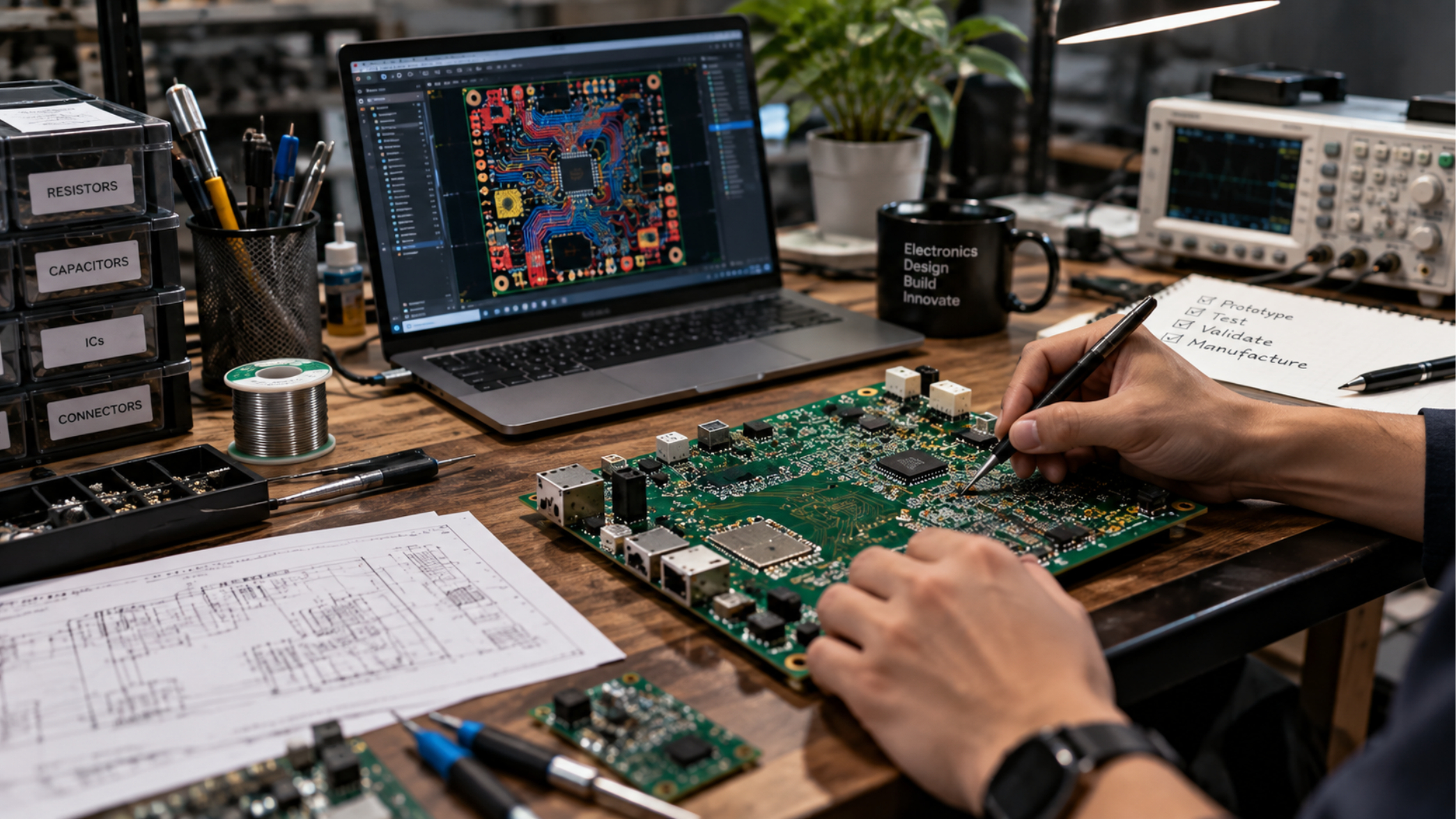

Multi-Layer & HDI Layout
Advanced stackup planning for microvia architectures, blind/buried vias, high-density BGA routing, and ultra-fine pitch components.

High-Speed Signal Integrity
Controlled differential impedance, length/phase matching, and jitter minimization for DDR4/5, PCIe Gen5/6, USB4, and HDMI lines.

Power Integrity & RF Layout
Low-noise PDN plane design, high-current thermal management, copper pour optimization, and RF microstrip antenna layouts.

EMI / EMC Mitigation
Strict design rules applied to minimize radiated emissions and susceptibility, ensuring pre-compliance for FCC, CE, and VCCI standards.
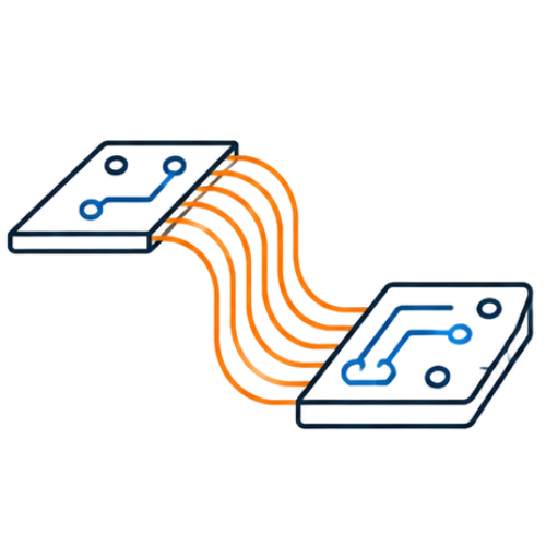
Rigid-Flex PCB Layout
Tailored layouts for dynamic bend requirements in wearables, medical technology, aerospace, and space-constrained enclosures.

DFM / DFA Optimization
Automated and manual design rule checks for fabrication and SMT assembly to maximize yield and reduce prototype iterations.